Intel Foundry and ASML reach a milestone of one million wafers processed on high-NA EUV scanners


In a significant development for the global semiconductor industry, Intel Foundry and ASML have announced that they have successfully processed more than one million 300mm wafers using High-Numerical Aperture (High-NA) Extreme Ultraviolet (EUV) lithography scanners. This milestone, disclosed during the recent SPIE Photomask Technology and EUV Lithography conference in Monterey, California, serves as a testament to the accelerated adoption of next-generation manufacturing technology by Intel and underscores the deepening strategic partnership between the two semiconductor titans.
The announcement represents more than just a production statistic; it signals a pivotal shift in the competitive landscape of chip manufacturing. For years, the industry has looked toward High-NA EUV as the essential bridge to the sub-2nm era of silicon fabrication. By achieving this volume of throughput, Intel is attempting to solidify its position as the premier pioneer in the deployment of this prohibitively expensive and technically complex equipment, directly addressing previous market perceptions that the company had fallen behind in the race for AI-centric hardware dominance.
The Significance of High-NA EUV Technology
To understand the weight of this achievement, one must grasp the technical leap High-NA EUV represents. Traditional EUV lithography, which uses a 0.33 numerical aperture, has been the workhorse for advanced node production over the past decade. However, as transistor densities have reached physical limits, the industry required a way to print smaller features with higher fidelity.
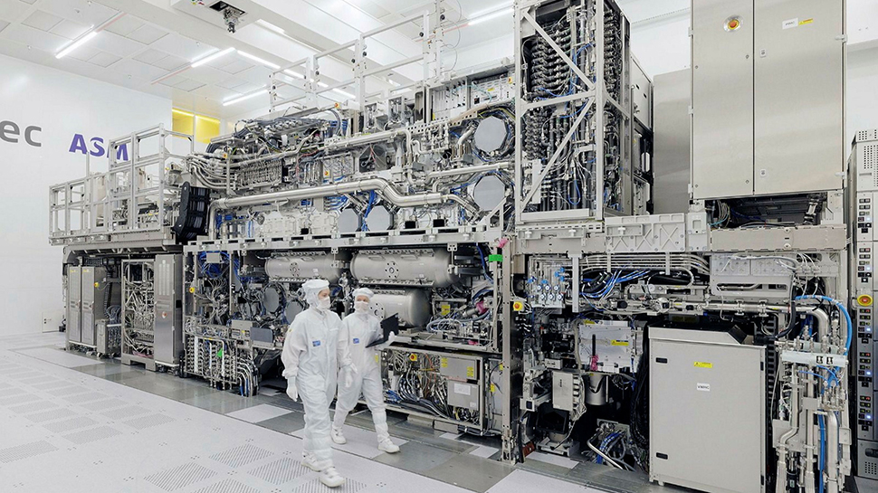
High-NA EUV, which utilizes a 0.55 numerical aperture, effectively doubles the resolution of the imaging process compared to its predecessor. This allows for the printing of smaller, more tightly packed transistors, which is critical for the next generation of artificial intelligence accelerators and high-performance computing (HPC) processors. Each scanner, such as the ASML EXE:5000 series, is a marvel of engineering, priced at roughly $350 million. They are the most complex machines ever built for mass production, requiring years of installation and calibration.
Intel’s "one million wafer" figure encompasses a broad range of activities, including internal research and development, rigorous tool certification, and the ongoing volume production of its Core Ultra Series 3 processors, known internally as Panther Lake. While the announcement does not specify the exact split between experimental and commercial output, it confirms that Intel is the first company in the world to successfully integrate this technology into a live, high-volume production pipeline.
A Chronology of Strategic Investment
Intel’s aggressive pursuit of High-NA lithography is a core pillar of its IDM 2.0 strategy. The company’s commitment to this technology dates back several years, with Intel serving as the primary launch customer for ASML’s latest scanners.
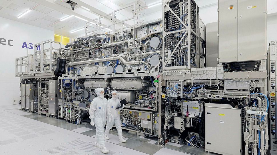
The timeline of this deployment has been closely watched by industry analysts:
- Late 2023 to Early 2024: Intel receives the first shipment of ASML’s High-NA EUV tools at its D1X development fab in Oregon. This initial phase was dedicated to machine calibration and foundational R&D.
- Mid-2024: The company transitions from early-stage testing to tool qualification for high-volume manufacturing (HVM).
- Late 2024 to 2025: Intel begins utilizing the machines for the initial production runs of its Panther Lake silicon.
- September 2026: The milestone of one million wafers is officially verified, marking the transition of the technology from a "bleeding-edge" experimental asset to a core production utility.
This timeline highlights a rapid ramp-up period that has surprised many industry observers, particularly those who questioned Intel’s ability to execute on its foundry roadmap following its well-documented struggles to compete with Nvidia in the AI GPU market.
Competitive Dynamics and Industry Context
The competitive landscape for semiconductor manufacturing is currently dominated by a handful of players: Intel, TSMC, Samsung, and SK Hynix. According to data provided by ASML, the total number of wafers exposed by all High-NA systems currently in operation across the industry stands at approximately 1.35 million.
This data point is striking: Intel’s share accounts for roughly 74% of all high-NA wafer throughput globally. While TSMC and Samsung have also acquired High-NA capacity, they have adopted a more cautious approach. TSMC, for instance, has publicly signaled that it does not intend to shift to high-volume manufacturing using High-NA EUV until approximately 2030, preferring to maximize the return on investment from its existing, highly optimized 0.33 NA EUV fleets.
This divergence in strategy creates a unique scenario. By "betting the farm" on the technology now, Intel is incurring immense capital expenditure costs, but it is also gaining a head start in process node maturity. If the yield rates for its High-NA production lines continue to stabilize, Intel may find itself with a significant lead in energy efficiency and transistor density, providing a tangible edge when competing for foundry contracts from companies like Nvidia or Apple, or when designing its own next-generation silicon.
Financial and Market Implications
The recent surge in Intel’s stock, which has climbed nearly 155% year-to-date, is partially attributed to this technological progress. The company’s foundry business is increasingly seen as a viable alternative for US-based chip production, a narrative supported by federal interest and investment.
Furthermore, the involvement of major industry players like Nvidia—who have shown increased interest in the foundry’s capabilities—suggests that the market is beginning to price in the success of Intel’s manufacturing turnaround. For investors, the "one million wafer" milestone serves as tangible evidence that the massive capital outlays are yielding physical, usable results.
However, risks remain. The semiconductor industry is notoriously cyclical, and the cost of maintaining and operating High-NA EUV infrastructure is astronomical. If the demand for AI-specific chips or advanced consumer processors plateaus, the heavy depreciation costs associated with these machines could weigh on Intel’s balance sheet. Furthermore, the company must prove that it can scale this technology to higher volumes while maintaining competitive yields across its entire product portfolio.
Future Outlook and Technical Challenges
Looking ahead, the focus for Intel and ASML will shift from initial throughput to yield optimization and cost-per-wafer reduction. As Greet Storms, ASML’s head of High-NA product management, noted, the industry is currently managing ten active systems across four major customers. With three additional systems in the process of installation, the total global capacity is expected to grow significantly over the next eighteen months.
For Intel, the challenge is twofold. First, it must continue to refine the patterning processes that take advantage of the 0.55 NA optics to ensure that the chips produced are not only advanced but also commercially viable at scale. Second, it must continue to market its foundry services to external partners, proving that its internal success with Panther Lake can be replicated for third-party clients.
The collaboration between Intel and ASML is fundamentally a high-stakes gamble on the future of Moore’s Law. By pushing the boundaries of what is physically possible in lithography, both companies are attempting to sustain the pace of innovation that has defined the digital age. Whether this million-wafer milestone is viewed as the beginning of a dominant era for Intel or merely an expensive early-mover hurdle will be determined by the company’s performance in the next two fiscal years.
For now, the industry has its answer: the age of High-NA EUV has arrived, and for the moment, Intel is leading the charge. The implications of this lead will likely reverberate through the semiconductor supply chain for the remainder of the decade, potentially reshaping the balance of power between the world’s most influential technology corporations.