Microsoft Unveils Significant EDA Performance Gains with New Azure Cobalt 200 Infrastructure


The semiconductor industry is currently navigating a period of unprecedented complexity, where the demand for specialized silicon to power artificial intelligence and massive cloud-scale systems has pushed traditional design methodologies to their limits. Every custom chip developed by Microsoft originates within the rigorous, compute-intensive environment of Electronic Design Automation (EDA). These workflows involve massive simulation sweeps, complex verification regressions, and memory-heavy physical signoff runs. Today, Microsoft has announced a pivotal evolution in this process: the deployment of its custom Azure Cobalt 200 compute infrastructure, built on the Arm Neoverse CSS V3 architecture. Early performance evaluations indicate that this new hardware delivers between 1.30x and 4.15x the performance of its predecessor, the Cobalt 100, across a wide spectrum of silicon design tasks.
The Evolution of Cloud-Based Silicon Design
Historically, the semiconductor industry relied on static, on-premise x86 server farms. These environments were frequently oversized to accommodate "peak" design cycles—such as the final weeks before a tapeout—leading to significant periods of underutilization and capital inefficiency. The migration to cloud-based EDA represents more than just a shift in location; it represents a fundamental change in resource management. By leveraging Microsoft Azure, engineering teams can now access virtually limitless scale, allowing them to spin up thousands of cores for an overnight regression test and scale back immediately upon completion.

The introduction of the Cobalt 200 virtual machine instances marks the next phase of this transition. Microsoft’s internal silicon engineering teams have been utilizing these instances to optimize the design of their own proprietary chips. The architecture of the Cobalt 200, which features dedicated 3MB L2 caches per core and high provisioned memory bandwidth, is specifically engineered to address the common bottlenecks in EDA tools, such as memory contention and inter-process communication overhead.
Chronology of Infrastructure Development
The development of the Cobalt series is part of a multi-year strategy by Microsoft to vertically integrate its cloud infrastructure. The journey began with the conceptualization of custom, Arm-based silicon designed specifically to maximize the efficiency of cloud-native workloads.
- Phase 1 (Cobalt 100): Microsoft introduced its first-generation Cobalt chips, establishing a foundation for cloud-based silicon development. These chips were designed to handle general-purpose cloud workloads but were also immediately put to use in internal EDA environments to prove the viability of Arm-based architectures for heavy-duty design work.
- Phase 2 (Performance Benchmarking): Throughout the development lifecycle of the Cobalt 200, Microsoft conducted rigorous benchmarking. Unlike standard enterprise software, EDA tools are highly sensitive to CPU architecture, cache hierarchy, and instruction set optimizations. By testing tools from Cadence, Synopsys, and Siemens, Microsoft sought to ensure that its hardware could support the most demanding verification suites without requiring modifications to the software stack.
- Phase 3 (General Availability): With the recent validation of the Cobalt 200, Microsoft is now opening these capabilities to external Azure customers, marking the transition from an internal optimization project to a public-facing cloud service.
Technical Performance Metrics and Comparative Analysis
To quantify the leap in performance, Microsoft subjected the Cobalt 200 to a battery of tests that mimic the real-world conditions of a modern chip development project. The testing focused on peak throughput per logical core, a metric that is critical for CAD managers who must plan the duration of nightly regressions.
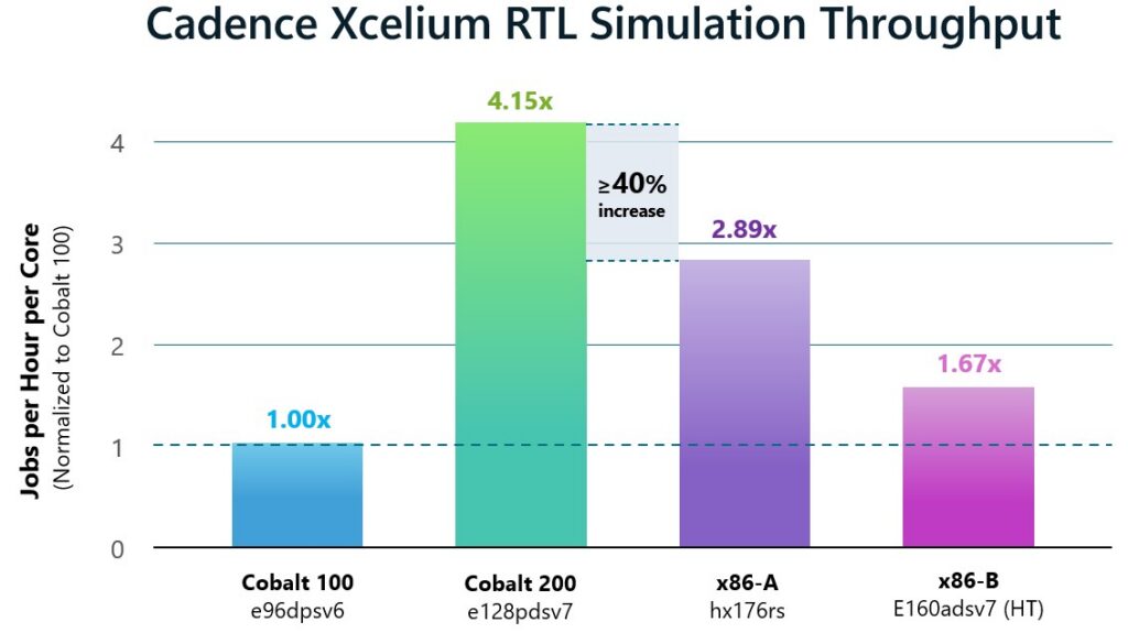
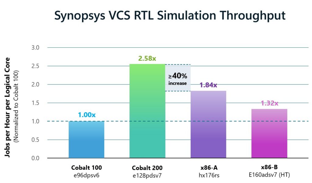
In the realm of digital simulation, which includes tools like Cadence Xcelium and Synopsys VCS, the Cobalt 200 demonstrated substantial advantages. For RTL simulation—a process that consumes the bulk of compute resources during the verification phase—the Cobalt 200 achieved more than 40% higher throughput per logical core than any other system tested, including previous Cobalt generations and competitive x86-based configurations.
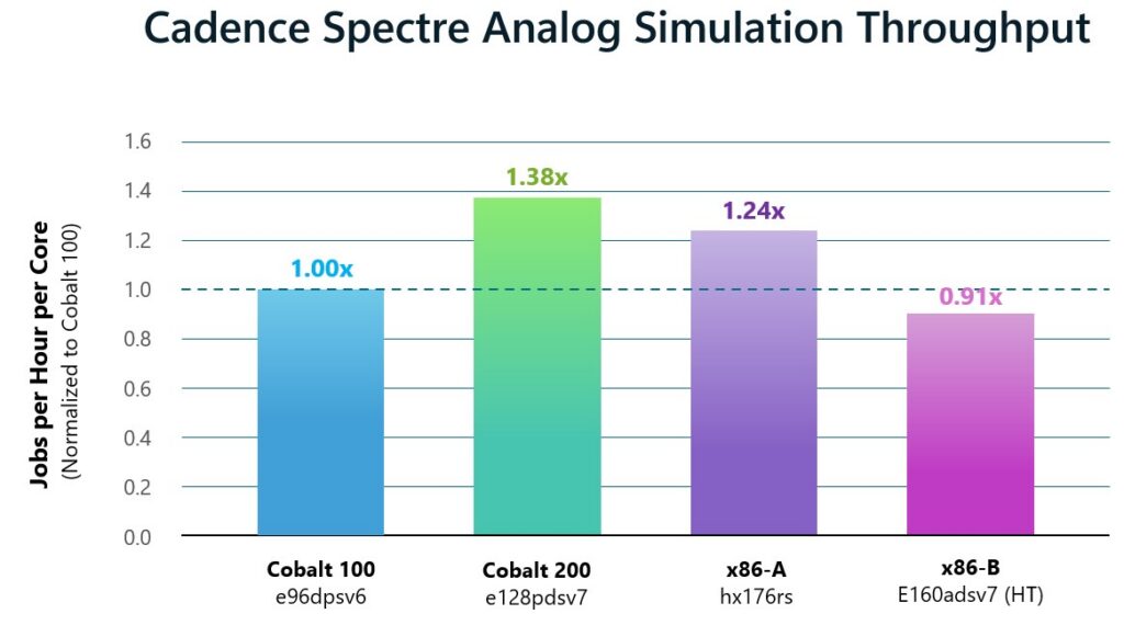
The performance gains were similarly striking in analog and mixed-signal simulation. Cadence Spectre, which relies heavily on multi-threaded performance, saw a 38% increase in throughput compared to the Cobalt 100. This is a critical finding, as analog design is notoriously difficult to parallelize, and the improvements in cache efficiency within the Cobalt 200 architecture directly correlate to these faster simulation times.
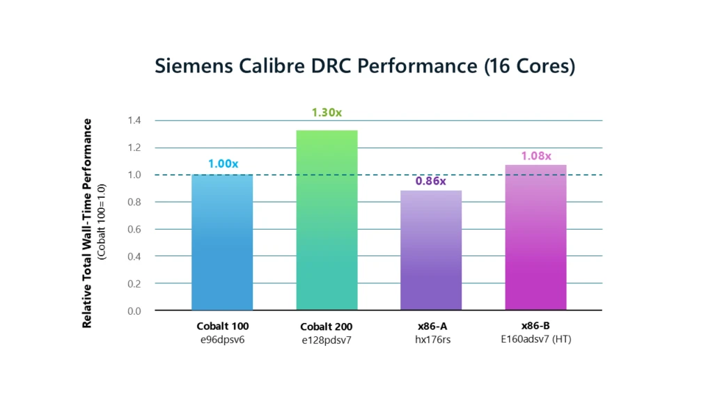
Physical verification, specifically the Siemens Calibre DRC (Design Rule Check), saw a 23% reduction in wall-clock time. This is perhaps the most tangible benefit for hardware engineers; shorter DRC runs allow for faster iterations on physical layouts, effectively shortening the time to tapeout. Furthermore, Synopsys PrimeTime, the industry standard for static timing analysis, recorded a 2x throughput improvement over the Cobalt 100, highlighting the effectiveness of the Cobalt 200’s memory architecture in handling the massive data structures inherent in timing analysis.
The Role of Ecosystem Partners
A critical component of this rollout is the seamless compatibility with existing EDA software. By ensuring that tools like Cadence Xcelium, Synopsys VCS, and Siemens Calibre ran without modification, Microsoft has removed the "friction cost" that often prevents companies from migrating to new hardware architectures.
Industry leaders have responded favorably to these results. Paul Cunningham, Senior Vice President and General Manager of the System Verification Group at Cadence, noted that the collaboration on Cobalt spans multiple generations of Azure silicon. He emphasized that the qualification of Cadence workflows on Cobalt 200 provides semiconductor teams with unprecedented flexibility in how they scale their compute resources.
Craig Johnson, Vice President of Cloud Solutions at Siemens EDA, echoed these sentiments, highlighting the growing pressure on engineering teams to accelerate development cycles. "Executing Siemens EDA solutions on Microsoft Azure Cobalt 200 provides an efficient, scalable platform for demanding verification and signoff workloads," Johnson stated.
From the Synopsys side, Sanjay Bali, Senior Vice President of EDA Product Management and Strategy, pointed out that the performance gains are not just theoretical but are directly impacting the design of future AI silicon. The 2x per-core throughput improvement in PrimeTime is a testament to the symbiotic relationship between the hardware being designed and the hardware being used to design it.
Broader Implications for the Semiconductor Industry
The implications of these advancements are twofold. First, for semiconductor firms, the ability to leverage such high-performance infrastructure in the cloud means that even smaller design houses can now afford the compute capacity previously reserved for the industry’s largest players. This democratizes the design process, potentially lowering the barrier to entry for innovative chip startups.
Second, the "virtuous cycle" mentioned by Microsoft is significant. By using its own custom hardware to design the next generation of its custom hardware, Microsoft is creating a feedback loop that accelerates innovation. Each generation of Cobalt chips benefits from the insights gained by the EDA workloads run on the previous generation. As these workloads scale, Microsoft gains granular data on where bottlenecks exist, allowing for iterative improvements in memory bandwidth, cache size, and core interconnects.
Furthermore, the shift to Arm-based cloud infrastructure is part of a wider industry trend. As x86 architectures face challenges in terms of power-to-performance efficiency, Arm-based chips—which have dominated the mobile market for years—are proving to be highly effective in the data center. The success of the Cobalt 200 in complex EDA environments signals a maturation of the Arm ecosystem in the high-performance computing (HPC) space.
Strategic Outlook and Next Steps
As the Cobalt 200 enters general availability, the next phase for Microsoft involves broadening workload coverage. While the current results are highly positive for digital, analog, and physical verification, the company is continuing to work with EDA partners to tune performance across the entire design flow.
For CAD managers and semiconductor architects, the choice of cloud infrastructure is no longer just a matter of cost-per-hour; it is a strategic decision that directly influences the speed of product delivery. The performance deltas provided by the Cobalt 200 suggest that moving EDA workflows to specialized, cloud-native hardware is no longer an optional optimization, but a necessary step for teams looking to remain competitive in an increasingly fast-paced and complex silicon design landscape. As Microsoft continues to iterate on its Azure infrastructure, the industry will likely see further convergence between the silicon being designed and the cloud environments that enable that design, setting the stage for even more efficient, high-performance computing systems in the years to come.