NASA Engineering and Safety Center Issues Technical Bulletin Addressing Ceramic Chip Resistor Fractures in Printed Circuit Board Assemblies

The NASA Engineering and Safety Center (NESC) has released a critical technical bulletin, TB-26-10, following the investigation of rare but significant structural failures in thick-film chip resistors utilized in mission-critical hardware. While chip resistors are ubiquitous throughout NASA’s diverse portfolio—ranging from deep-space probes to earth-orbiting satellites—these components are generally considered highly reliable. However, the discovery of transverse substrate cracking during environmental acceptance testing has prompted a comprehensive review of assembly practices, specifically regarding how ceramic-bodied components interact with the mechanical stresses inherent in printed circuit board (PCB) assembly.
The investigation, spearheaded by the Langley Research Center under the technical guidance of Joel W. Sills, highlights a specific failure mode: transverse fractures occurring across the short axis of resistors. These failures, which presented as intermittent open-circuit faults during thermal cycling, have led to a re-evaluation of best practices for board-level design and assembly.
Chronology of the Discovery and Investigation
The issue came to light during routine environmental acceptance testing of printed circuit board assemblies. The failure pattern was consistent across two identical boards: the resistors failed specifically during the thermal cycling phase, which followed a prior vibration testing protocol. Engineers observed that the resistors functioned normally at room temperature but exhibited intermittent electrical open circuits when the hardware reached elevated thermal dwell points.
Upon physical inspection, it was determined that the resistors had suffered a clean, transverse fracture at their mid-span, running parallel to the terminations. The placement of these components was notable; both failed resistors were located in similar proximity to the edge of the printed circuit boards.
Initial diagnostic efforts were focused on the possibility of a systemic defect within the component supply chain. Because both failures occurred on identical boards and involved resistors from the same procurement lot, investigators first hypothesized that a latent manufacturing defect might be to blame. The lot was checked against the stringent MIL-PRF-55342 procurement specification. However, after extensive review and supplementary testing, the NESC concluded that the resistors were manufactured to standard, compliant specifications and exhibited no inherent material flaws that would suggest a "bad batch" scenario.
Failure Analysis and Technical Root Cause
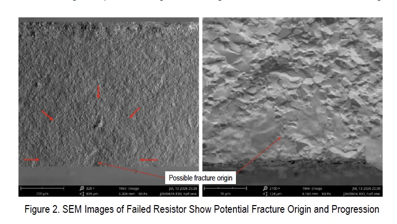
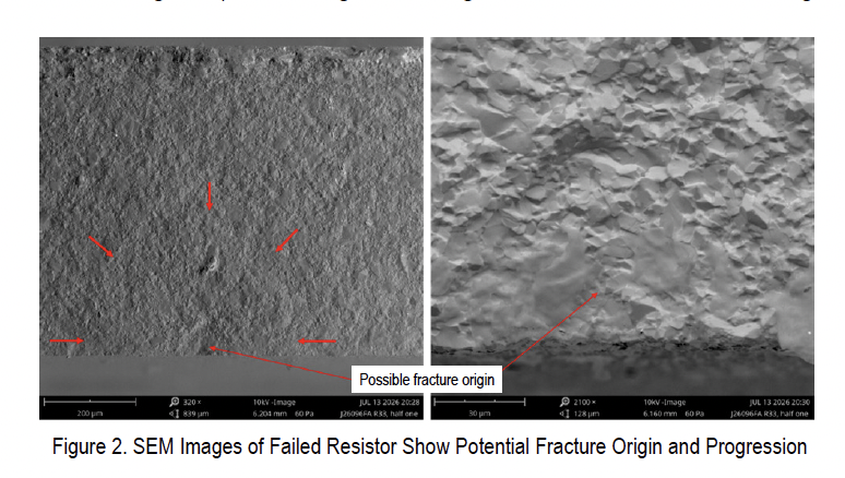
To determine why these specific resistors failed while others on the same board remained intact, the NESC conducted an independent failure analysis utilizing high-resolution scanning electron microscopy (SEM) and optical imaging.
The analysis ruled out cyclic fatigue as the primary driver. In typical vibration-related failures, one would expect to see signs of crack propagation and progression indicative of repeated mechanical stress cycles. Instead, the observed damage signatures were purely indicative of a sudden, bending-induced tensile failure. The crack morphology showed a straight, clean break, consistent with excessive force applied during board flexure.
The investigation concluded that the failures were mechanical rather than electronic. The "bending" force was likely introduced during the assembly or handling of the PCB. Components located near the board edge are particularly susceptible to stress when a board undergoes "bowing" or "twisting"—common phenomena that occur during the soldering process or when the board is fastened into a chassis. When the board flexes, the rigid ceramic substrate of the resistor, soldered firmly to the pads, cannot accommodate the deformation. Because the ceramic is brittle, it reaches its tensile limit and snaps.
Supporting Data and Environmental Factors
The environmental testing protocol that triggered these failures serves as a stress-test for the resilience of aerospace hardware. The combination of vibration—which can introduce initial micro-strains—followed by thermal cycling—which causes materials to expand and contract at different rates based on their coefficients of thermal expansion (CTE)—creates a "perfect storm" for brittle materials.
Data from the investigation suggests that several factors contributed to the stress concentration:
- Component Orientation: The physical alignment of the resistor relative to the board’s edge increased its vulnerability to bending moments.
- Solder Fillet Height: Excessive solder volume creates a rigid connection that prevents the component from "floating" or absorbing minor board strains, effectively coupling the resistor directly to the board’s deformation.
- Board Geometry: The proximity to the edge of the PCB meant the resistors were in a zone of maximum displacement during any board-level mechanical flexure.
Guidelines for Mitigation and Future Assembly
In light of these findings, the NESC has issued a set of revised guidelines for engineers and technicians involved in the assembly of space-grade electronics. The objective is to decouple the fragile ceramic components from the mechanical stresses inherent in PCB manufacturing and integration.
1. Strategic Component Placement
Designers are now advised to avoid placing large-footprint ceramic components near the edges of printed circuit boards. Edge zones are prone to higher levels of strain during mechanical fastening and thermal expansion, making them the least ideal locations for components with brittle substrates.
2. Finite Element Analysis (FEA) Integration
Before final board layouts are approved, engineers should employ FEA to model how the PCB will respond to both mechanical vibration and thermal cycling. By predicting areas of high stress or board "bowing," designers can relocate sensitive components to neutral zones where the board remains stable.
3. Controlled Solder Application
The NESC emphasizes the importance of controlling the solder fillet height. While robust soldering is necessary for electrical connectivity, an over-application of solder can make a component too rigid. Technicians are encouraged to follow strict IPC standards for solder volume to ensure that the connection is sufficient for current but allows for a minimal degree of mechanical compliance.
4. Enhanced Inspection Protocols
Inspection should go beyond simple electrical verification. High-magnification optical inspection is recommended post-assembly to detect micro-cracks that may not yet have caused an open circuit but are poised to fail under operational stress.
5. Functional Thermal Shock Testing
To identify latent issues before the hardware is integrated into a launch vehicle or satellite, the NESC recommends that environmental testing protocols include thermal shock cycles that specifically target the structural integrity of board-level components, rather than focusing solely on electrical functionality.
Broader Implications for Aerospace Engineering
The NESC bulletin serves as a reminder that even the most standardized, widely used components require rigorous attention to the physics of their installation. The move toward higher-density PCB designs, combined with the extreme environments of space flight, means that design margins are becoming increasingly narrow.
"The fact that these resistors met all military specifications underscores that this was not a failure of the component’s quality, but a failure of the design-to-assembly interface," notes a lead materials engineer familiar with the bulletin. "As we push for smaller, more efficient electronics, we are finding that the mechanical interaction between the PCB and the surface-mount component is just as critical as the circuitry itself."
The industry-wide implication is a shift toward a more holistic view of "packaging" for space electronics. The reliance on standard procurement specifications, while necessary, is no longer sufficient on its own. Engineers must integrate structural mechanics into the early design phase of PCB development. By recognizing the PCB not just as a circuit carrier, but as a dynamic mechanical structure that undergoes deformation, mission designers can prevent the premature failures that threaten the success of long-duration space missions.
As NASA continues to integrate more complex and miniaturized systems, the lessons from the TB-26-10 bulletin are expected to be incorporated into standard operating procedures across all centers. This proactive stance ensures that the high reliability expected of space-grade hardware is maintained, even as the constraints of size, weight, and power (SWaP) continue to evolve.
For contractors and aerospace firms following NASA standards, the bulletin acts as a mandatory update to their assembly manuals. By implementing these rigorous placement and inspection protocols, the agency aims to eliminate "bending-induced cracking" as a risk factor, ensuring that the critical electronic components powering the next generation of exploration remain robust from the cleanroom to the cosmos.